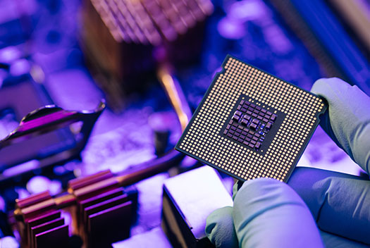
A crucial aspect in semiconductor manufacturing is an ultra-clean and particle-free production environment. Creation of these complex works of art requires the cleanest of environments, especially as the semiconductors get smaller and more powerful. A single speck of dust or a microscopic burr from a chemical vapor line would be catastrophic in the production process as the result would be to scrap the entire wafer and start over. Semiconductors are found in everyday items like computer CPUs, smartphones, refrigerators, televisions and LED bulbs to the most advanced computer systems in the world like missile guidance systems, the International Space Station, the world banking system, the Mars Rover, and more.
Semiconductor chips are manufactured by a multistep process involving chemical vapor deposition, photolithography, chemical stripping, and other processes to create engineered structures onto the surface of specially prepared silicon wafers. For the components in the gas delivery systems and in the photoresist systems, electropolished 316L/316 is the alloy of choice.
Electropolishing is essential for creating a smooth inner surface for tubing to be used in gas distribution systems. Electropolishing is an electrochemical process that strips away metallic impurities and smooths imperfections, leaving a much cleaner surface. This process is commonly used as a final step for metal parts utilized in these applications to create an ultraclean surface that resists corrosion.
So much technology depends on semiconductors. To create them, every step of the process requires the utmost cleanliness, unimpeded flow in the chemical distribution systems, and specific surface roughness requirements. Only electropolishing can meet all these criteria.